• KOREA
  • HOME
  • CONTACT US
  • SITEMAP
LM 디지털주식회사
  • Company
    • CEO Greeting
    • Company Overview
    • Philosophy
    • Organization
    • Major Customers
    • Introduction to workplaces
  • Business Description
    • Testing
    • Fixture
    • Laser Drill
    • Work process
  • SALES
    • Universal System
    • Flying Probe System
    • ECT PIN
images

business

PCB Electronical Testing

Verify

Bare Board Testing

Universal

35mil,50mil

Deadicate

compound

wireprobe

PCB Laser Drilling CO2

work process

design process

디자인공정
HOME> Business > Design Process
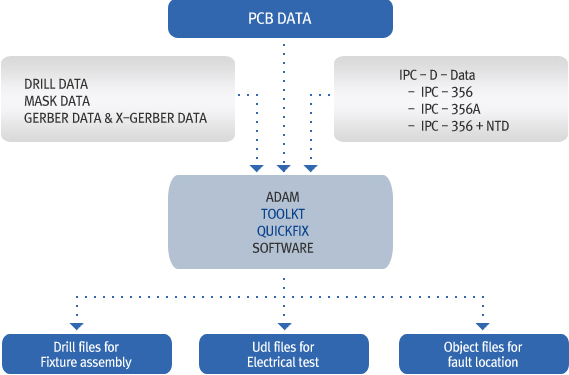
ADAM ll(Adapter Design & Artworks Manipulation ll)
for 
01 Input, Analysis and Translation of PCB data from the CAM station
02 Designing and building fixture
03 Electrical PCB testing
04 Fault location on PCB
05 Output of ,obj-, drill-and , udl files
06 Possible to input data formats are
- Gerber data , X-Gerber data
- dfp data (available early 1999)
- IPC-D356, IPC-D356A and IPC-D356A + NTD
 
ADAM ll SOFTWARE CONCEPT
           
  • Company
  • Location
headquartered 908-10hogye-dong,dongan-gu, anyang-si,gyeonggi-do,korea TEL 031.456.6171 FAX 031.456.6613 COPYRIGHT 2013 LM DIGLTAL COMPANY ALL RIGHTS RESERVED
atg LUTHER&MAELZER logo